
FBDIMM
What is FBDIMM?
A Fully Buffered Dual Inline Memory Module (FBDIMM) is a type of memory module in computer systems designed to enhance memory performance and capacity. It achieves this by connecting multiple memory modules to the memory controller via a serial interface, unlike traditional DRAMs (Dynamic Random Access Memory) that use a parallel bus architecture.
FBDIMMs have a serial interface between the memory controller and the advanced memory buffer (AMB), addressing the issues of signal deterioration and limited bandwidth in traditional systems.
The FBDIMM specification, like most RAM standards, was established by JEDEC (Joint Electron Device Engineering Council).
FBDIMM System Architecture
FBDIMM memory utilizes a bi-directional serial bus that routes through each memory module, rather than relying on a single bus where all modules transmit their data. Like PCI Express (Peripheral Component Interconnect Express) and other modern serial technologies, FBDIMM sends memory data in packets, with the flow precisely managed by AMB chips within each module. In contrast, traditional memory modules use a parallel 'stub' connection, where each module has its own set of links to the memory controller. High memory densities can strain the memory controller, leading to errors and delays, forcing a compromise between small, fast memory or large, slower, but more accurate memory—neither of which is optimal for modern servers.
Advantages of FBDIMM Memory Technology
-
Simplifying new memory technologies and reducing transition costs: The AMB chip used in FBDIMM memory serves as a buffer, facilitating the transmission of commands from the memory controller to the DRAM. It essentially handles serial-to-parallel data conversion, allowing existing DRAM chips to be utilized directly on FBDIMMs. This design approach eases the adoption of new memory technologies, as it doesn't require changes from memory chip manufacturers. This challenge was necessary when transitioning from SDRAM to DDR or Rambus, which required manufacturer support.
-
Large memory access and low fault-tolerant signal interference: A platform utilizing FBDIMM technology can support up to six channels, with each channel accommodating eight DIMMs and each DIMM supporting two ranks. Currently, the maximum capacity per FBDIMM is 4GB, allowing the platform to theoretically reach up to 192GB of memory. Intel's 5000 series chipsets, for example, support up to four channels, each with four DIMMs, potentially allowing for 64GB of memory. However, most released servers are equipped with eight DIMMs, limiting maximum memory to 32GB. Despite this, data is transmitted in orderly packets, minimizing errors and signal interference, which ensures that servers can fully utilize high-speed DDR2 memory while maintaining access to the substantial memory capacity required for complex applications like databases.
-
Bandwidth Advantages of Multi-Channel Serial: The bi-directional serial interface in FBDIMM modules allows for simultaneous data transmission and reception, effectively eliminating the read-to-write latency seen in traditional memory. The interface's bandwidth ranges from 3.2GB/s to 4.8GB/s, depending on the DDR2 memory type used (DDR2-533, 667, or 800). Due to the lower pin count and superior data handling capabilities of these serial links compared to conventional memory buses, more channels can be incorporated into a single memory controller. This gives entry-level servers and high-end desktops with four FBDIMM modules, each on a separate channel, a significant bandwidth advantage over traditional dual-channel memory controllers that support two DDR2 DIMMs per channel. However, while the initial latency of serial memory may be higher than that of conventional memory setups, this drawback diminishes during continuous data transfers, where the serial interface's faster speed and bi-directional nature provide a clear performance edge.
-
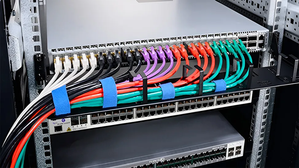
Simplify Motherboard Wiring and Reduce Development Costs: Each FBDIMM channel utilizes just 69 signal lines, significantly simplifying routing compared to the 240 signal lines needed for the current parallel DDR2 channel. The previous figure illustrates the cabling for the DDR2 memory board (on the left) and the FBDIMM memory board (on the right). In the DDR2 Registered DIMM board, a single channel necessitates two routing layers for signal cables and an additional layer for power supply. In contrast, a motherboard designed for FBDIMMs requires only two routing layers for two channels, which also includes a power supply. This simplification will ease motherboard cabling, lessen design complexity, shorten the product development timeline, and enhance productivity.

Key Technologies of FBDIMMs
Frequency
FB-DIMM technology uses various frequency parameters, including clock frequency, DRAM clock frequency, DRAM data transfer rate, channel transfer rate, and channel unit interval. These parameters are interrelated. The external clock source provides a lower frequency reference clock for both the AMB and the host. The AMB then multiplies this clock to produce the needed signal for DRAM. The DRAM data transfer rate is twice the DRAM clock signal frequency, following the double data rate (DDR) mode. The channel speed is based on the Unit Interval (UI), the average time for power conversions in the FBD channel, and is six times the DRAM data transfer rate.
For example, if the external clock source runs at 166 MHz (6 ns), the AMB outputs a 333 MHz (3 ns) signal for the DRAM, and the FBD channel unit interval is 250 ps (PicOS®econds). This setup results in a channel speed of 4.0 Gbps.
AMB Interface
The main parts of the FBDIMM are the Advanced Memory Buffer (AMB) and its connections, which include two FBD link interfaces, one DDR2 channel interface, and one SMBus interface. The FBDIMM uses a daisy chain setup, allowing up to eight DIMMs per channel.
Each FBDIMM channel has two-way communication: a southbound link for sending commands, addresses, and data to the DRAM, and a northbound link for reading data from the DRAM. The southbound link has 10 lanes, while the northbound link has 14 lanes.
The DDR2 channels of the AMB connect directly to DDR2 SDRAM, supporting two ranks per channel. Each rank has eight banks, enabling 16 row/column requests, 64 data lines, and eight parity lines.
The AMB’s SMBus interface allows system access to configuration registers without going through the FBD link. This interface operates at 100 kHz and is useful for system startup and fault diagnosis.
The AMB also provides error correction without extra processor or memory controller load. It can detect and fix faulty data paths, reducing errors and allowing parallel read and write operations. This makes it easier to use different memory controller chips interchangeably.
Frame and Bandwidth
The southbound and northbound interfaces differ in data frame formats and capacities. The northbound read transmission rate is twice that of the southbound write rate, reflecting the higher frequency of read operations.
The southbound interface uses 10 pairs of differential signal lines (20 physical lines) with a 10x12 frame format, transmitting 10x12 bits per DRAM clock cycle. A southbound frame has three command slots, with slot A carrying the command and address, and slots B and C transmitting commands or writing data. Write data is sent via the Command+Wdata frame, transmitting 72 bits of data each channel. Two frames transfer 144 bits, aligning with the data transferred in a single DRAM clock cycle, achieving one burst 8 transfer or two consecutive burst 4 transfers, totaling 72 bytes (64 bytes of data plus 8 bytes of ECC data). The peak throughput of southbound connections is half that of a single DRAM channel, e.g., 2.133 GB/s for DDR2 533 DRAM.
The northbound interface has 14 pairs of differential signal lines (28 physical lines) in a 14x12 frame format, transmitting 14x12 bits per DRAM clock. A northbound frame carries 144 bits (18 bytes), matching the ECC data capacity in a single DRAM clock cycle. Like the southbound interface, the northbound achieves one burst 8 transfer or two consecutive burst 4 transfers, also providing 72 bytes of data. The peak theoretical throughput of the northbound link is equal to that of a single DRAM channel, e.g., 4.267 GB/s for DDR2 533 DRAM.
The combined peak throughput of a single FBD channel (northbound + southbound) is 1.5 times that of a single DRAM channel, reaching 6.4 GB/s for the FBD-533 channel compared to 4.267 GB/s for DDR2 533.
FBD Channel Delay
When the Variable Read Latency function is not enabled, the latency for any FBDIMM in the FBD channel is consistent with that of other FBDIMMs. As additional DIMMs are incorporated into the FBD channel, the latency for reading data from each DIMM increases accordingly. This increase occurs because the FBD channel comprises multiple point-to-point internal interconnect DIMMs, requiring memory requests to traverse N-1 buffers to reach the Nth buffer. Consequently, the idle read latency in a 4-DIMM channel configuration is greater than that in a 1-DIMM configuration. The Variable Read Latency function helps to decrease the latency for DIMMs that are closer to the host.
Hot-swap
The FBDIMM channel lacks a mechanism to detect the addition of a new FBDIMM. The system's memory controller must initialize the newly added FBDIMM. Following this, a hot-add reset is conducted, allowing the new FBDIMM to operate alongside the existing one. Before an FBDIMM is removed, the host sends a quick reset command to the last FBDIMM to prepare it for removal.
It is important to note that even though the FBDIMM is hot-swappable, the power supply to the FBDIMM slot will be cut off during the installation or removal of the FBDIMM. If this function is implemented, the system must take this into account.
You might be interested in

Email Address


PoE vs PoE+ vs PoE++ Switch: How to Choose?
May 30, 2024


-